ZHCSOV0E March 2005 – November 2021 UCD7100
PRODUCTION DATA
- 1 特性
- 2 應用
- 3 說明
- 4 Revision History
- 5 說明(續(xù))
- 6 Device Comparison Table
- 7 Pin Configuration and Functions
- 8 Specifications
- 9 Detailed Description
- 10Application and Implementation
- 11Power Supply Recommendations
- 12Layout
- 13Device and Documentation Support
- 14Mechanical, Packaging, and Orderable Information
封裝選項
請參考 PDF 數(shù)據(jù)表獲取器件具體的封裝圖。
機械數(shù)據(jù) (封裝 | 引腳)
- PWP|14
散熱焊盤機械數(shù)據(jù) (封裝 | 引腳)
- PWP|14
訂購信息
8.5 Electrical Characteristics
VDD = 12 V, 4.7-μF capacitor from VDD to GND, TA =
TJ = –40°C to 105°C, (unless otherwise noted).
| PARAMETER | TEST CONDITIONS | MIN | TYP | MAX | UNIT | |
|---|---|---|---|---|---|---|
| SUPPLY SECTION | ||||||
| Supply current, OFF | VDD = 4.2 V | 200 | 400 | μA | ||
| Supply current | Outputs not switching IN = LOW | 1.5 | 2.5 | mA | ||
| LOW VOLTAGE UNDER-VOLTAGE LOCKOUT | ||||||
| VDD UVLO ON | 4.25 | 4.5 | 4.75 | V | ||
| VDD UVLO OFF | 4.05 | 4.25 | 4.45 | |||
| VDD UVLO hysteresis | 150 | 250 | 350 | mV | ||
| REFERENCE / EXTERNAL BIAS SUPPLY | ||||||
| 3V3 initial set point | TA = 25°C | 3.267 | 3.3 | 3.333 | V | |
| 3V3 over temperature | 3.234 | 3.3 | 3.366 | |||
| 3V3 load regulation | ILOAD = 1 mA to 10 mA, VDD = 5 V | 1 | 6.6 | mV | ||
| 3V3 line regulation | VDD = 4.75 V to 12 V, ILOAD = 10 mA | 1 | 6.6 | |||
| Short circuit current | VDD = 4.75 to 12 V | 11 | 20 | 35 | mA | |
| 3V3 OK threshold, ON | 3.3 V rising | 2.9 | 3.0 | 3.1 | V | |
| 3V3 OK threshold, OFF | 3.3 V falling | 2.7 | 2.8 | 2.9 | ||
| INPUT SIGNAL | ||||||
| HIGH, positive-going input threshold voltage (VIT+) | 1.65 | 2.08 | V | |||
| LOW negative-going input threshold voltage (VIT-) | 1.16 | 1.5 | ||||
| Input voltage hysteresis, (VIT+ – VIT-) | 0.6 | 0.8 | ||||
| Frequency | 2 | MHz | ||||
| CURRENT LIMIT (ILIM) | ||||||
| ILIM internal current limit threshold | ILIM = OPEN | 0.466 | 0.50 | 0.536 | V | |
| ILIM maximum current limit threshold | ILIM = 3.3 V | 0.975 | 1.025 | 1.075 | V | |
| ILIM current limit threshold | ILIM = 0.75 V | 0.700 | 0.725 | 0.750 | ||
| ILIM minimum current limit threshold | ILIM = 0.25 V | 0.21 | 0.23 | 0.25 | mV | |
| CLF output high level | CS > ILIM , ILOAD = -7 mA | 2.64 | V | |||
| CLF output low level | CS ≤ ILIM, ILOAD = 7 mA | 0.66 | ||||
| Propagation delay from IN to CLF | IN rising to CLF falling after a current limit event | 10 | 20 | ns | ||
| CURRENT SENSE COMPARATOR | ||||||
| Bias voltage | Includes CS comp offset | 5 | 25 | 50 | mV | |
| Input bias current | –1 | uA | ||||
| Propagation delay from CS to OUTx | ILIM = 0.5 V, measured on OUTx, CS = threshold + 60 mV | 25 | 40 | ns | ||
| Propagation delay from CS to CLF | ILIM = 0.5 V, measured on CLF, CS = threshold + 60 mV | 25 | 50 | |||
| CURRENT SENSE DISCHARGE TRANSISTOR | ||||||
| Discharge resistance | IN = low, resistance from CS to AGND | 10 | 35 | 75 | ? | |
| OUTPUT DRIVERS | ||||||
| Source current(1) | VDD = 12 V, IN = high, OUT = 5 V | 4 | A | |||
| Sink current(1) | VDD = 12 V, IN = low, OUT = 5 V | 4 | ||||
| Source current(1) | VDD = 4.75 V, IN = high, OUT = 0 | 2 | ||||
| Sink current(1) | VDD = 4.75 V, IN = low, OUT = 4.75 V | 3 | ||||
| Rise time, tR(1) | CLOAD = 2.2 nF, VDD = 12 V | 10 | 20 | ns | ||
| Fall time, tF(1) | CLOAD = 2.2 nF, VDD = 12 V | 10 | 15 | |||
| Output with VDD < UVLO | VDD = 1.0 V, ISINK = 10 mA | 0.8 | 1.2 | V | ||
| Propagation delay from IN to OUTx, tD1 | CLOAD = 2.2 nF, VDD = 12 V, CLK rising | 20 | 35 | ns | ||
(1) Ensured by design. Not 100% tested in production.
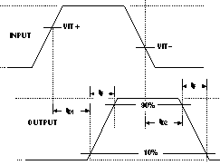
Figure 8-1 Timing Diagram